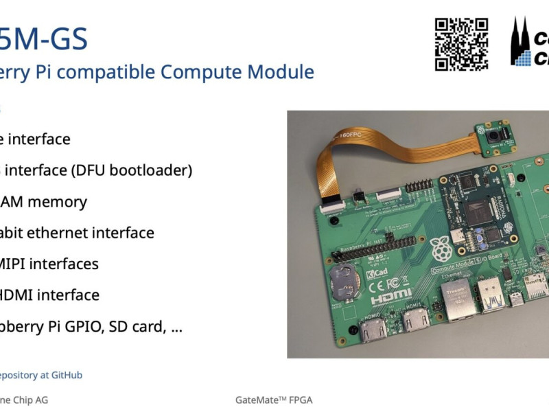
At the start of 2023. NLnet decided to sponsor the development of BB3-CM4.
Once we have finished creating base board we decided to create STM32 H7 SoM board
https://nlnet.nl/project/BB3-CM4
Why?
Main purpose of this CM4 compatible board is to have a STM32 H7 SoM for Envox BB3
Staring up with a pinout
The current STM32H7 pinout looks like this:

With this pinout, we have covered all peripherals that are currently available on Enovx EEZ BB3 (Bench Box 3) https://www.envox.eu/eez-bb3/
CubeMX IOC
Next in line was creating of CubeMX project as MCUs are not as easy as FPGA and most pins have a dedicated purpose. Envox helped me with creating a complete pinout as they are more experienced in STM32 projects...
Except that SoM is easier to replace and switch to the new board main difference between the F7 board that Envox already has in BB3 and this H7 board is connected to an LCD screen - H7 now has a screen connected over DSI. This H7 only provides one DSI data line.

PCB - Kicad
As always we are using free and opensource tool KiCad!
I have taken schematics from the BB3 project, and just made some changes, mostly removing peripherals that the SoM board does not need as we have everything on the baseboard.
The main part of the work was to route the remaining elements on the PCB - board has 6 layers but signals are routed only on 3 layers Signal/GND/Signal/Power/GND/Signal.

Board 3D View


Assembled board

Problems
Once I had assembled the board I tried to connect with STLINK, but it did not work, so I asked Envox if they were noticing something strange in schematics.
They first found this, but it should not be so problematic.
This problem sometimes occurs in Kicad - if you drag a component sometimes wires can be automatically connected to some wire that it is crossing!

As this board was a little bit different than the F7 board (it has DSI) I needed to do a little bit of rework around the power supply pins, and while I was doing that I created a big problem. I have connected the VCC pin to the GND pin :(
Oh nooo, as signal lines on that part of the schematics are connected in the middle board layer there is no way out.
We need to fix this and order a new board.

Oh wait - there is a "destructive" solution to our problem
After some thinking, I have noticed that maybe there is a way out of this. I need to break connections between the left and right parts of the board and there is only one VIA that connects that. So if I remove that VIA, and one more line that is on the bottom layer I will be able to separate GND and VCC, so let's drill a hole in the middle of the board!!
Yeah!!!

I think I did manage to damage one signal line that is connected to the top layer - I have checked and that is OE_SYNC - I think it is not super important.
I may also damage the middle signal DOUT3, but this is also not a super important signal.

Happy board
After loading the initial FW that is not doing anything but has all peripherals initialized I have noticed that the board is happy and consuming around 100mA

BB3 with H7 board

Next steps
It will take some time, but the next step is to check all parameters one by one, the first thing we need to check will be a connection to SDRAM.
Board repository
https://github.com/intergalaktik/bb3-cm4/tree/main/EEZ_BB3_CM4_H7
Contact
Radiona/intergalaktik discord: https://discord.gg/qwMUk6W
Envox discord: https://discord.gg/btKVC5sedG
Many thanks to NLnet for sponsoring our work!
By: Goran Mahovlić
This project is funded by NLnet https://nlnet.nl/project/BB3-CM4/
This project was funded through the NGI0 Entrust Fund, a fund established by NLnet with financial support from the European Commission's Next Generation Internet programme, under the aegis of DG Communications Networks, Content and Technology under grant agreement No 101069594.


You might also like
-
Goran Mahovlic @ BalCCon2k24
- Written by Intergalaktik
- Published on
-
eBadge ZigZag @ BSides Zagreb 2026
- Written by Intergalaktik
- Published on
-
FPGA ULX5M presented @ CERN
- Written by Intergalaktik
- Published on
-
ZigZag e-badge on OSHWA Show & Tell
- Written by Intergalaktik
- Published on
-
ULX5M presented @ BalCCon2k25
- Written by Intergalaktik
- Published on


